When smaller means better: analyzing how device scaling enhances memory performance
Researchers reveal that shrinking ferroelectric tunnel junctions delivers key advantages for next-generation non-volatile memory technologies
Shrinking ferroelectric tunnel junctions can significantly boost their performance in memory devices, as reported by researchers from Science Tokyo. The team fabricated nanoscale junctions directly on silicon substrates and analyzed conduction mechanisms across a wide temperature range and multiple device scales. They found that smaller junction areas produced much larger resistance contrasts between the ‘ON’ and ‘OFF’ states, demonstrating that miniaturization could directly improve both efficiency and reliability in future non-volatile memory technologies.
Understanding Key Design Parameters for Ferroelectric Tunnel Junction Memory Devices

The rapid rise of artificial intelligence (AI), edge computing, and the Internet of Things (IoT) has created unprecedented demand for faster, denser, and more energy-efficient data storage. To meet these requirements, memory devices must operate at extremely high speeds while consuming minimal power. However, conventional flash memory, which stores data using electric charge, is approaching its physical and scaling limits. As device dimensions continue to shrink, charge-based storage suffers from reliability and leakage issues, driving researchers to explore alternative memory concepts.
Against this backdrop, ferroelectric tunnel junctions (FTJs) have emerged as a promising candidate for next-generation non-volatile memories. Instead of storing charge, FTJs encode information using the direction of electric polarization in an ultrathin ferroelectric layer—typically only a few nanometers thick. This polarization state directly modulates the quantum-mechanical tunneling probability of electrons, resulting in two distinct resistance states (ON and OFF). While FTJs are widely regarded as attractive for low-power memory applications, experimental evidence clarifying how device miniaturization influences their performance, particularly in CMOS-compatible material systems, has remained limited.
In a recent study, a research team led by Professor Yutaka Majima from the Materials and Structures Laboratory (MSL), Institute of Innovative Research (IIR), Institute of Science Tokyo (Science Tokyo), Japan, in collaboration with Professor Hiroshi Funakubo from the School of Materials and Chemical Technology, Science Tokyo, and Associate Professor Seiichiro Izawa from MSL, IIR, Science Tokyo, addressed this critical gap through a systematic investigation of nanoscale FTJs fabricated directly on silicon substrates. Their paper, published online in Volume 18, Issue 5 of the journal Nanoscale on January 2, 2026, examines how shrinking the junction area affects tunneling electroresistance (TER) and charge-transport mechanisms over a broad temperature range.
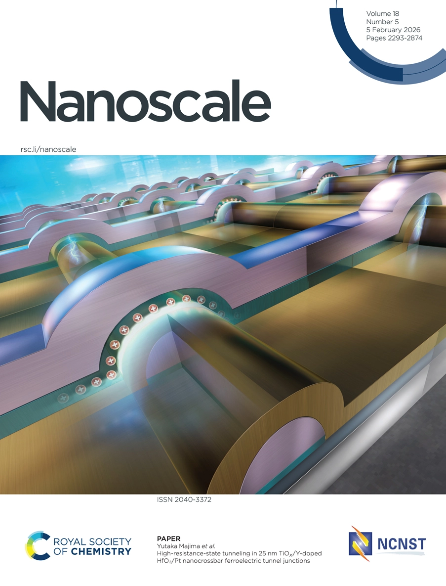
The team focused on hafnium-oxide (HfO2)-based ferroelectrics, which are considered more compatible with advanced semiconductor manufacturing than conventional perovskite materials. Using an original electron-beam lithography approach, the team fabricated ‘nanocrossbar-type’ FTJs. Each device consists of a titanium/titanium oxide top electrode, a 2–3 nm-thick yttrium-doped HfO2 ferroelectric barrier, and a platinum bottom electrode formed on a silicon oxide/silicon substrate. “The nanocrossbar structure enables a compact, highly ordered array that supports two-terminal addressing and extremely high cell density, making it well suited for scalable ferroelectric memory architectures,” explains Majima.
Electrical measurements revealed that electrons tunnel directly through the ferroelectric barrier in both the ON and OFF states, even at cryogenic temperatures. This behavior contrasts with many earlier FTJ studies, where leakage currents and thermally activated transport dominated the high-resistance (OFF) state. Most notably, the team found that reducing the junction area dramatically enhances the TER ratio—the relative resistance difference between polarization states that determines how clearly stored data can be distinguished. The smallest nanocrossbar FTJ, with a junction width of just 25 nm, achieved a remarkably high TER ratio of 2,200, exceeding that of larger devices by more than an order of magnitude.
These findings challenge the conventional assumption that device performance inevitably degrades as dimensions shrink. Instead, the study demonstrates that aggressive scaling can be a powerful strategy for improving memory characteristics. “Our key finding—smaller FTJ devices exhibit substantially larger TER ratios—provides an important design guideline for realizing ultra-high-density, low-power, and three-dimensionally integrated memory architectures, which are essential for future memory technologies,” concludes Majima.
Overall, this work establishes a clear experimental foundation for scaling FTJs and provides a practical pathway toward next-generation non-volatile memories that can support emerging applications in AI, portable electronics, and IoT.

Reference
- Authors:
- Zhongzheng Sun1, Yoshiko Nakamura2, Kazuki Okamoto2, Seiichiro Izawa1, Hiroshi Funakubo2, and Yutaka Majima1*
*Corresponding author - Title:
- High-resistance-state tunneling in 25 nm TiOx/Y-doped HfO2/Pt nanocrossbar ferroelectric tunnel junctions
- Journal:
- Nanoscale, 18, 2293-2874, (2026)
- DOI:
- 10.1039/D5NR04010H
- Affiliations:
- 1Institute of Integrated Research, Institute of Science Tokyo, Japan
2School of Materials and Chemical Technology, Institute of Science Tokyo, Japan
Related articles
Further information
Professor Yutaka Majima
Institute of Integrated Research, Institute of Science Tokyo
- majima@msl.titech.ac.jp
Contact
Public Relations Division, Institute of Science Tokyo
- media@adm.isct.ac.jp
- Tel
- +81-3-5734-2975